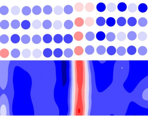
Researchers from the Electronic Ceramics Department, the Department for Nanostructured Materials (Jožef Stefan Institute) and the Department of Materials Chemistry (National Institute of Chemistry), i.e., A. Bencan, G. Drazic, M. Makarovic, H. Ursic, M. Komelj and T. Rojac, published a study in Nature Communications titled “Domain-wall pinning and defect ordering in BiFeO3 probed on the atomic and nanoscale” (https://www.nature.com/articles/s41467-020-15595-0). Using a combined characterization of BiFeO3 on the nano and atomic scale, the study reveals a pinning mechanism associated with conductive domain walls (DWs), whose origin lies in the dynamic coupling of the p-type defects gathered in the DW regions with the DW displacements under applied electric field. The authors confirmed that the degree of defect ordering at the walls, which affect the DW local structure and conductivity, can be tuned by the cooling rate used during the annealing. The results are useful in the design of the DW architecture and dynamics for emerging nanoelectronic and ferroelectric bulk applications.
